The use of this site and the content contained therein is governed by the Terms of Use. When you use this site you acknowledge that you have read the Terms of Use and that you accept and will be bound by the terms hereof and such terms as may be modified from time to time.
All text, graphics, audio, design and other works on the site are the copyrighted works of nasscom unless otherwise indicated. All rights reserved.
Content on the site is for personal use only and may be downloaded provided the material is kept intact and there is no violation of the copyrights, trademarks, and other proprietary rights. Any alteration of the material or use of the material contained in the site for any other purpose is a violation of the copyright of nasscom and / or its affiliates or associates or of its third-party information providers. This material cannot be copied, reproduced, republished, uploaded, posted, transmitted or distributed in any way for non-personal use without obtaining the prior permission from nasscom.
The nasscom Members login is for the reference of only registered nasscom Member Companies.
nasscom reserves the right to modify the terms of use of any service without any liability. nasscom reserves the right to take all measures necessary to prevent access to any service or termination of service if the terms of use are not complied with or are contravened or there is any violation of copyright, trademark or other proprietary right.
From time to time nasscom may supplement these terms of use with additional terms pertaining to specific content (additional terms). Such additional terms are hereby incorporated by reference into these Terms of Use.
Disclaimer
The Company information provided on the nasscom web site is as per data collected by companies. nasscom is not liable on the authenticity of such data.
nasscom has exercised due diligence in checking the correctness and authenticity of the information contained in the site, but nasscom or any of its affiliates or associates or employees shall not be in any way responsible for any loss or damage that may arise to any person from any inadvertent error in the information contained in this site. The information from or through this site is provided "as is" and all warranties express or implied of any kind, regarding any matter pertaining to any service or channel, including without limitation the implied warranties of merchantability, fitness for a particular purpose, and non-infringement are disclaimed. nasscom and its affiliates and associates shall not be liable, at any time, for any failure of performance, error, omission, interruption, deletion, defect, delay in operation or transmission, computer virus, communications line failure, theft or destruction or unauthorised access to, alteration of, or use of information contained on the site. No representations, warranties or guarantees whatsoever are made as to the accuracy, adequacy, reliability, completeness, suitability or applicability of the information to a particular situation.
nasscom or its affiliates or associates or its employees do not provide any judgments or warranty in respect of the authenticity or correctness of the content of other services or sites to which links are provided. A link to another service or site is not an endorsement of any products or services on such site or the site.
The content provided is for information purposes alone and does not substitute for specific advice whether investment, legal, taxation or otherwise. nasscom disclaims all liability for damages caused by use of content on the site.
All responsibility and liability for any damages caused by downloading of any data is disclaimed.
nasscom reserves the right to modify, suspend / cancel, or discontinue any or all sections, or service at any time without notice.
For any grievances under the Information Technology Act 2000, please get in touch with Grievance Officer, Mr. Anirban Mandal at data-query@nasscom.in.
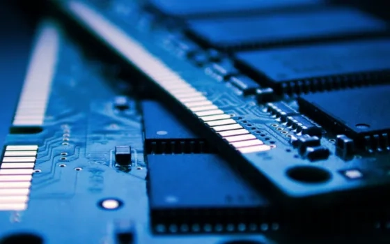
In the current era of digital revolution, there is a growing demand for high capacity, high bandwidth, low cost, error free, low power semiconductor memories that occupies minimal area. The existing memory types and technologies are being improved further and new types and technologies are being introduced. DRAM is commonly used in smartphones, tablets, PCs, data centers, cloud, graphics, consumer products, automobiles, etc. The 5G, AI, AR/VR and IoT technologies are also major drivers of the DRAM market.
DRAM
The older DRAMs were asynchronous DRAMs, in which there were no system clocks to synchronize memory accesses. The data transfer between the synchronous system bus and asynchronous memory bus was not efficient and resulted in longer delays. In synchronous DRAMs, the system clock coordinates the memory accesses and provides higher performance than asynchronous DRAMs. Today, synchronous DRAMs are widely used instead of asynchronous DRAMs. DRAMs are protected from bit-flip errors using ECC.
SYNCHRONOUS DRAMs
SDR SDRAM
Single data rate SDRAM can transfer single data per clock cycle. Typical SDR SDRAM clock rates are 66, 100 and 133 MHz, respectively denoted as PC66, PC100 & PC133 and operate at a voltage of 3.3V.
DDR SDRAM
The Double Data Rate SDRAM interface makes higher transfer rates possible by more strict control of the timing of the electrical data and clock signals. The interface transfers data on both positive and negative edge of clock to double data bus bandwidth without a corresponding increase in clock frequency. The name “double data rate” refers to the fact that a DDR SDRAM with a certain clock frequency achieves nearly twice the bandwidth of an SDR SDRAM running at the same clock frequency.
Prefetch architecture in DDR SDRAMs allows to fetch multiple words with a single address request. For example, when a memory read occurs to a row, the prefetch buffer also fetches a set of adjacent words without the need of individual column addresses. The prefetch buffer depth is related to DRAM core frequency and DRAM IO frequency. This feature significantly improves performance due to the principle of locality. Each generation of SDRAM has a different prefetch size. For example, DDR SDRAM’s prefetch buffer size is 2n i.e., 2 data words per memory access.
DDR SDRAM
Clock frequency (MHz)
Prefetch size
Data rate (MT/s)
Voltage
DDR1
100-200
2n
200-400
2.5-2.6
DDR2
200-5331/3
4n
400- 10662/3
1.8
DDR3
400- 10662/3
8n
800- 21331/3
1.5/1.35
DDR4
800-1600
8n
1600-3200
1.2/1.05
DDR5
1600-3600
8n
3200-7200
1.1
Table: Basic specification difference between different generations of DDR SDRAMs. Source
LPDDR SDRAM
Low-Power Double Data Rate SDRAM consumes less power due to various features like low I/O supply voltage, Temperature Compensated Self Refresh, Partial Array Self Refresh, Deep Power Down etc. that make the technology more appropriate for the mobile application and is targeted for mobile computers and devices such as mobile phones. Older variants are also known as Mobile DDR and abbreviated as mDDR. LPDDR technology standards are developed independently of DDR standards. In the “E” versions or the enhanced versions of the specifications, memory array is overclocked for a 33% performance boost.
The supply voltages of different generations of LPDDRs are generally lesser than that of DDRs. This reduces power consumption significantly since switching power is directly proportional to CV2f where C is the Capacitance, V is the Voltage swing, f is the operating frequency. In the Temperature Compensated Self Refresh (TCSR), the refresh rate changes in response to the on-chip temperature sensor, .i.e., at low temperatures, the refresh oscillator frequency decreases and saves power. Partial Array Self Refresh is a specific mode in which refresh is carried out in banks where data retention is required, thus reducing self-refresh current and thereby saves power. The Deep power down mode is the least power mode in which all the memory contents are sacrificed.
DDR SDRAM
Clock frequency (MHz)
Prefetch size
Data rate (MT/s)
Command/Address bus
Voltage
LPDDR1
200, 266.7(LPDDR-1E)
2n
400, 533.3(LPDDR-1E)
19 bits, SDR
1.8
LPDDR2
400, 533.3(LPDDR-2E)
4n
800, 1067(LPDDR-2E)
10 bits, DDR
1.2, 1.8
LPDDR3
800, 1067(LPDDR-3E)
8n
1600, 2133(LPDDR-3E)
10 bits, DDR
1.2, 1.8
LPDDR4
1600
16n
3200
6 bits, SDR
1.1,1.8
LPDDR4X
2133
16n
4267
6 bits, SDR
0.6, 1.1, 1.8
LPDDR5
3200
16n
6400
7 bits, DDR
0.5,1.05, 1.8
LPDDR5X
4267
16n
8533
7 bits, DDR
0.5,1.05, 1.8
Table: Basic specification difference between different generations of LPDDR SDRAMs. Source
GDDR SDRAM
Graphics DDR SDRAM are specifically designed for high bandwidth applications like GPUs. They have wider bus to provide higher bandwidth and performance. GDDR3 has much the same technological base as DDR2, but the power and heat dispersal requirements have been reduced and it has simplified cooling systems. GDDR4 SDRAM introduced DBI (Data Bus Inversion) and Multi-Preamble to reduce data transmission delay. GDDRs are expensive.
High Bandwidth Memory (HBM) is a high speed memory interface for 3D-stacked SDRAM, used in conjunction with high-performance graphics accelerators, network devices, high-performance datacenter, AI ASICs etc. HBM has higher bandwidth, low power consumption and smaller form factor. This is achieved by stacking up to eight DRAMdies vertically and this also helps to shorten the datapath. HBM memory bus is much wider as compared to other DRAM types. For example, An HBM stack of four DRAM dies with each die having two channels of 128 bits wide provides a total width of 1024 bits. The dies within the stack are interconnected by through-silicon vias (TSVs) and microbumps.
Since there are larger number of connections to the HBM than other DRAM types, new method of connection is used. As HBM occupies less space, it can be placed near GPU or CPU. The memory stack can be connected to the memory controller on a GPU or CPU through a substrate like interposer. Alternatively, the memory die could also be stacked directly on the GPU or CPU chip.
In February 2021, Samsung announced the development of HBM with processing-in-memory (PIM). A DRAM-optimized AI engine is placed inside each memory bank to enable parallel processing and minimize data movement. Samsung claims this will deliver twice the system performance and reduce energy consumption by more than 70%, while not requiring any hardware or software changes to the rest of the system.
CHALLENGES AND SOLUTIONS
Efficient architectural techniques are necessary to make better use of the available memories. To increase the capacity of DRAMs, memory cells are scaled down to smaller dimensions. Smaller transistors switch faster, use less energy and are cheaper to make. To overcome scaling challenges, we need innovative processes and material development. Efficient memory interface technologies can play an important role to meet growing performance requirements.
Compute Express Link (CXL)
CXL is a highly efficientmemory interface technology that eliminates proprietary memory interconnects and enables different processors to share a pool of memory. CXL is an open standard for high-speed central processing unit (CPU)-to-device and CPU-to-memory connections.
The CXL standard defines three separate protocols:
CXL.io - based on PCIe 5.0 with a few enhancements, it provides configuration, link initialization and management, device discovery and enumeration, interrupts, DMA, and register I/O access using non-coherent loads/stores.
CXL.cache - allows peripheral devices to coherently access and cache host CPU memory with a low latency request/response interface.
CXL.mem - allows host CPU to coherently access cached device memory with load/store commands for both volatile (RAM) and persistent non-volatile (flash memory) storage.
CXL is designed to support three primary device types:
Type 1 (CXL.io and CXL.cache) – specialised accelerators (such as smart NIC) with no local memory. Devices rely on coherent access to host CPU memory.
Type 2 (CXL.io, CXL.cache and CXL.mem) – general-purpose accelerators (GPU, ASIC or FPGA) with high-performance GDDR or HBM local memory. Devices can coherently access host CPU’s memory and/or provide coherent or non-coherent access to device local memory from the host CPU.
Type 3 (CXL.io and CXL.mem) – memory expansion boards and storage-class memory. Devices provide host CPU with low-latency access to local DRAM or non-volatile storage.
Persistent Memory
Persistent memory (PMEM) is a solid-state high-performance byte-addressable non-volatile memory device that resides on the DRAM bus and provides nearly the same speed and latency as DRAM. They are much larger in capacity, cheaper and durable when compared to DRAM, and are also cacheable. They are ideal for applications like big data analytics, metadata servers, AI, IoT technologies etc. that require frequent access to large, complex data sets and are sensitive to downtime due to system crashes or power failures. If the working datasets can fit within the capacity of persistent memory and DRAM, the system performance increases significantly.
CONCLUSION
DRAM technology is evolving at a fast pace due to the immense growth of memory-intensive applications. Semiconductor giants have already started working on next-generation memory standards with very high data rates and those are expected to hit the market in the coming years.
That the contents of third-party articles/blogs published here on the website, and the interpretation of all information in the article/blogs such as data, maps, numbers, opinions etc. displayed in the article/blogs and views or the opinions expressed within the content are solely of the author's; and do not reflect the opinions and beliefs of NASSCOM or its affiliates in any manner. NASSCOM does not take any liability w.r.t. content in any manner and will not be liable in any manner whatsoever for any kind of liability arising out of any act, error or omission. The contents of third-party article/blogs published, are provided solely as convenience; and the presence of these articles/blogs should not, under any circumstances, be considered as an endorsement of the contents by NASSCOM in any manner; and if you chose to access these articles/blogs , you do so at your own risk.
In today’s fast-paced legal landscape, efficiency and accuracy are not just desirable—they are essential. Alternative Dispute Resolution (ADR) mechanisms like arbitration have gained significant traction for offering faster and more cost-effective…
As we move deeper into the AI-powered era of mobile innovation, 2025 stands out as a defining year for Android app development. With Android powering over 72% of global smartphones, the ecosystem is evolving faster than ever—driven by emerging…
In an era where digital experiences are becoming the norm, interacting with an AI chatbot no longer feels robotic. From retail support to mental health coaching, modern AI chatbots can carry on conversations that feel genuinely human. But how did we…
Q2 2025 saw USD 1.7 billion inflows, 29% rise compared to Q1 2025. Mumbai & Bengaluru together drove 39% of the investment inflows in H1 2025.
After a steady start in the first quarter, institutional investments in the Indian real…
The great travel reboot: Generative AI’s role in ending the planning chaos
Written by Sankar Subramaniam, Global Travel Industry Research Lead, Accenture
A few weeks ago, I tried to plan a short getaway. I opened my laptop and suddenly found…
In H12025, a leading product company announced plans to cut nearly 8,000 jobs as it ramped up AI-based automation efforts. Another big tech laid off its experienced IT position holder along with a significant amount of human capital. Read any recent…