In today’s world, hardware platforms are growing in complexity and reducing the time to market for these platforms is key to capturing the market segment. Gone are the days when the hardware was considered as a critical piece; customers now expect the board to be delivered as a package containing world-class hardware infrastructure with reliable & robust software to run complex applications. This brings the need to equip the engineers with the right set of tools to get them started to meet these challenges and work effectively.
Software development starts early, right at the pre-silicon stage, using reference boards or FPGA platforms. Having a sophisticated debug infrastructure is an important part of development of these software systems. The infrastructure helps in two aspects 1) in recreating some of the corner case scenarios while testing the software which otherwise might not have been possible and 2) any issues that are seen in the software can be recreated and isolated providing engineers the capability to quickly debug the software.
For this debugging phase, a well-known interface that many engineers rely on, is the JTAG. Manufacturers provide JTAG to empower engineers with complete access to test and program integrated circuits.
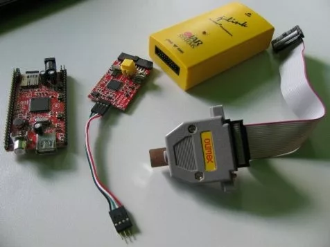
Different types of JTAG debuggers
There are several powerful tools provided by third party vendors capitalizing the JTAG interface for debugging. However, these devices do not come cheap and investing in such a tool for multiple hardware platforms is sure to shoot up your overall costs exponentially. So, is there a possibility to get similar flexibility at a fraction of the cost? This blog intends to address just this, by introducing the JTAG interface as well as providing a low-cost solution to engineers by combining OpenOCD software for debugging via JTAG.
What is JTAG ?
JTAG is an IEEE standard (1149.1) developed in the 1980s to solve electronic boards manufacturing issues. It is primarily used for verifying designs and testing printed circuit boards after manufacture. In short, it is a hardware interface to communicate directly with the chips on a board.
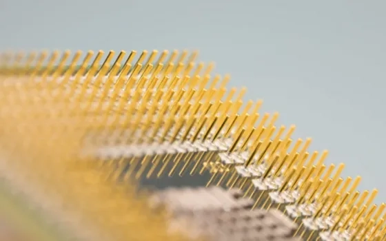
In the past, tests on PCBs (Printed Circuit Boards) were done through a system called bed-of-nails. PCB was designed with several test points to be connected to this test board to perform checks.
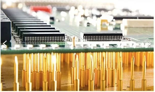
Testing via a bed of nails
A few novel uses of a JTAG are
- Connect to a hardware device to read / write from its memory
- Dump RAM and gain access to sensitive data such as passwords and cryptographic keys
- Inject instructions directly into the pipeline of the target chip
- Activate peripherals and change their behavior, such as setting or resetting an I/O pin
- Access Flash Memory to update and or modify the firmware of a device
JTAG Architecture
Basic architecture of the JTAG circuitry consists of a set of Data Registers (DR), set of Instruction Registers (IR), a finite state machine (FSM) to arbitrate data and four pin serial interface. Discussing and detailing the FSM is beyond the scope of this blog.
The JTAG specification IEEE 1149.1 specifies not only the signals but how the “State Machine” embedded in the TAP (Test Access Port) Controller of a device must behave. So, the JTAG interface requires a minimum of 4 pins to communicate with the chip. These signals, and silicon logic that connects and controls them, are collectively referred to as the Test Access Port, or TAP controller.
- TCK (Test Clock) – The actual clock speed is not specified in the JTAG standard. The TAP controller accepts its speed from the outside device controlling JTAG.
- TMS(Test Mode Select) – Used as an input into the TAP controller
- TDI (Test Data In) – A pin to feed data into the chip and what the chip does with them is irrelevant to JTAG.
- TDO (Test Data Out) -The pin for data coming out of the chip.
- [Optional]TRST(Test Reset)- This optional signal is used to reset JTAG to a known good state.
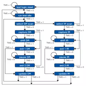
JTAG state machine
Note that
- data is read into and out of the TDI and TDO pins while the state machine is in the Shift-IR or Shift-DR states.
- The IR (Instruction Register) and DR (Data Register) are like function calls.
- The value in IR is the “function” and the value in DR is the “argument”.
- The JTAG specification doesn’t define what the “functions” should be, that’s up to the manufacturer.
Interesting thing to note is that keeping TMS high for more than 5 clock cycles brings the state machine from any state back to the test logic reset state. Thus, a separate TRST pin is optional and not necessary.
TAP(Test Access Port)
ANSI/IEEE Standard 1149.1-1990, (Standard Access Port and Boundary-Scan Architecture) defines test logic that can be included on an integrated circuit to provide standardized approaches to testing the component itself or the interconnections between components on a printed circuit board.
The test logic allows test instructions and test data to be fed to a component, and upon execution of an instruction, allows the results to be read out and observed. All instructions, test data, and results are communicated in serial format. The test logic defined by the standard consists of a chain of boundary-scan cells and test support logic, which are accessed through the TAP inputs.
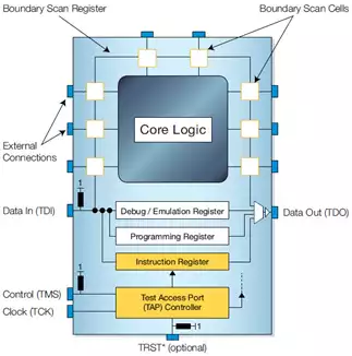
Schematic Diagram of JTAG enabled Device
TAP (Test Access port) can be considered as the controller which initiates different internal tests, provides access to internal registers based upon the instruction registers assigned to it..
Every TAP is expected to have an IDCode Register holding a unique Identity Code to differentiate and recognize it. The primary step in JTAG debugging is to identify the TAP connected to the interface and use the appropriate IR/DR (Instruction/Data Registers) set to access the internal chip resources. One of the most powerful tools you can pair with JTAG, to unlock the true potential of this interface via automation is OpenOCD. Automation coupled with remote access to various stations remotely is a key requirement here and OpenOCD provides just that — an intuitive interface that can be tailored to your needs and different SoC architectures.
OpenOCD (Open On-Chip Debugger)
OpenOCD is the only Open Source debugging software tool/repository (knowledge base) for a variety of chips and interfaces. This can (when paired with a JTAG interface device) manipulate the JTAG’s TAP controller on a target device to send bits to it (via the state machine above), which the chip will interpret as valid commands.
Support for OpenOCD requires certain information regarding the device to properly sequence JTAG signals for communication and thus we need to write a configuration file capturing the device architecture. Config files for many of the most common chip types are included within the OpenOCD and new ones need to be written for custom designer chips.
OpenOCD lets you perform all the basic operations you would expect like pause, step through an operation, inspect memory, write bytes directly into memory, set watch-points, add breakpoints, and more complex operations like inject code into the process or process memory. This technique is called “Hardware Based Software Debugging” as we are manipulating the hardware to perform traditional software debugging tasks. For a new core which is not supported, the framework has to be modified to support these operations.
As mentioned earlier, the software is open source and available for anyone to use as required. Ignitarium has been providing custom JTAG + OpenOCD solutions for chip design / verification teams (of various chip manufacturers) to run their validation tests on their chips having non-standard complex JTAG daisy chains.
One of the main challenges with ASIC / SoC having multicore architecture is the debugging of its various blocks. For a bringup of new silicon, as most of you are aware, the first trusted tool is the JTAG, which in its traditional CLI form can be time consuming and cumbersome to work with. OpenOCD coupled with JTAG can considerably reduce the time for the entire activity. However, this support also requires adding the respective debug structures to be separately integrated into the OpenOCD software layer so as to enable normal and complex debug setup for these chips in an automated fashion.
References
- JTAG Primer
- Coresight debug Architecture
- Technical guide to JTAG
- OpenOCD Source Repo
- JTAG Fundamentals
This blog originally appeared on Ignitarium.com's Blog Page.


